Public Peter Vanoppen EUV Products and Business opportunity ASML Investor Day Veldhoven, The Netherlands November 14, 2024 Executive Vice President and Head of Business Line 0.55 NA EUV Small Talk 2024 Teun van Gogh Executive Vice President and Head of Business Line 0.33 NA EUV Exhibit 99.4
Public Key messages • EUV has reached high-volume manufacturing maturity providing a solid foundation for continued innovation. • The NXE:3800E offers a 38% improvement in productivity and 13% in overlay, with additional productivity and overlay improvements planned for the NXE:4000F and beyond. • The imec ASML High NA EUV lab opened in June, and all EUV customers have exposed critical layers. The data prove the capability of the system in lowering costs by 20-35% for critical layers compared to 0.33 NA, by dose reduction, enabling single exposure and 2D layout designs. • The first High NA EUV systems are operational at a customer, marking a key milestone in adoption of High NA EUV. • In the future both 0.33 NA and 0.55 NA EUV systems will be used for critical exposures. The EUV roadmap for the next decade includes the introduction of a high productivity platform and will enable affordable scaling for both 0.33 NA, 0.55 NA and potentially Hyper NA. • The growing installed base opportunity will be leveraged with a value- based service model in combination with productivity and performance upgrades.
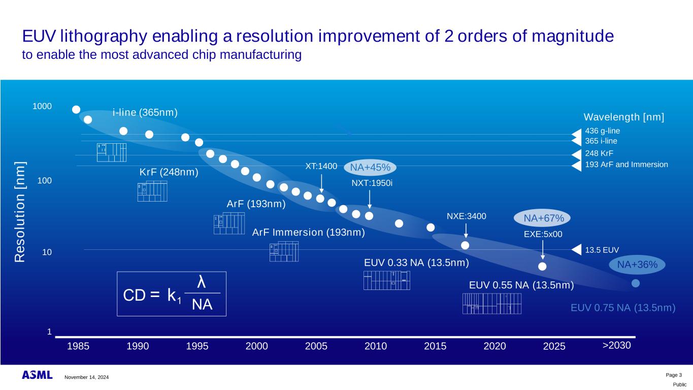
Public 13.5 EUV Wavelength [nm] 436 g-line 365 i-line 248 KrF 193 ArF and Immersion EUV lithography enabling a resolution improvement of 2 orders of magnitude to enable the most advanced chip manufacturing Page 3 R e s o lu ti o n [ n m ] 10 100 1000 1 1985 1990 1995 2000 2005 2010 2015 2020 2025 >2030 ArF (193nm) EUV 0.33 NA (13.5nm) EUV 0.55 NA (13.5nm) ArF Immersion (193nm) KrF (248nm) i-line (365nm) NA+67% NXT:1950i NXE:3400 EXE:5x00 XT:1400 NA+45% EUV 0.75 NA (13.5nm) NA+36% November 14, 2024
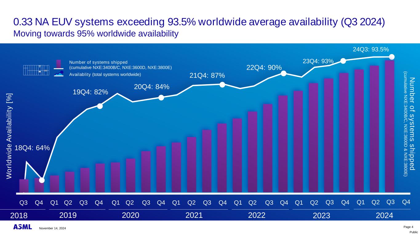
Public Page 4 20222018 24Q3: 93.5% 20202019 2021 Q1 Q2 Q3 Q4 Q1 Q2 Q3 Q4 Q1 Q2 Q3 Q4 Q1 Q2 Q3 Q4 2023 Q1 Q2 Q3 Q4 Q1Q4Q3 2024 Q2 W o rl d w id e A v a il a b il it y [ % ] 18Q4: 64% 19Q4: 82% 20Q4: 84% 21Q4: 87% 22Q4: 90% 23Q4: 93%Number of systems shipped (cumulative NXE:3400B/C, NXE:3600D, NXE:3800E) Availablity (total systems worldwide) Q3 Q4 N u m b e r o f s y s te m s s h ip p e d (c u m u la tiv e N X E :3 4 0 0 B /C , N X E :3 6 0 0 D & N X E :3 8 0 0 E )8545 53 55 62 76 923 8 11 5 12 7 0.33 NA EUV systems exceeding 93.5% worldwide average availability (Q3 2024) Moving towards 95% worldwide availability November 14, 2024
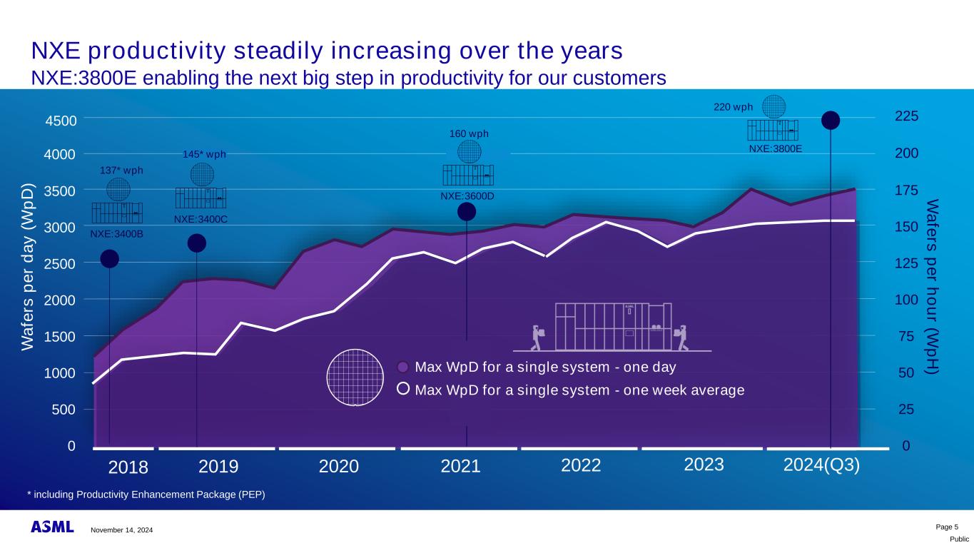
Public NXE productivity steadily increasing over the years NXE:3800E enabling the next big step in productivity for our customers Page 5 3500 3000 2500 2000 1500 1000 500 0 2018 20202019 2021 2022 2023 W a fe rs p e r d a y ( W p D ) 2024(Q3) 175 150 125 100 75 50 25 0 W a fe rs p e r h o u r (W p H ) NXE:3400B NXE:3400C NXE:3600D 200 225 NXE:3800E 4000 4500 Max WpD for a single system - one day Max WpD for a single system - one week average 220 wph 160 wph 145* wph 137* wph * including Productivity Enhancement Package (PEP) November 14, 2024
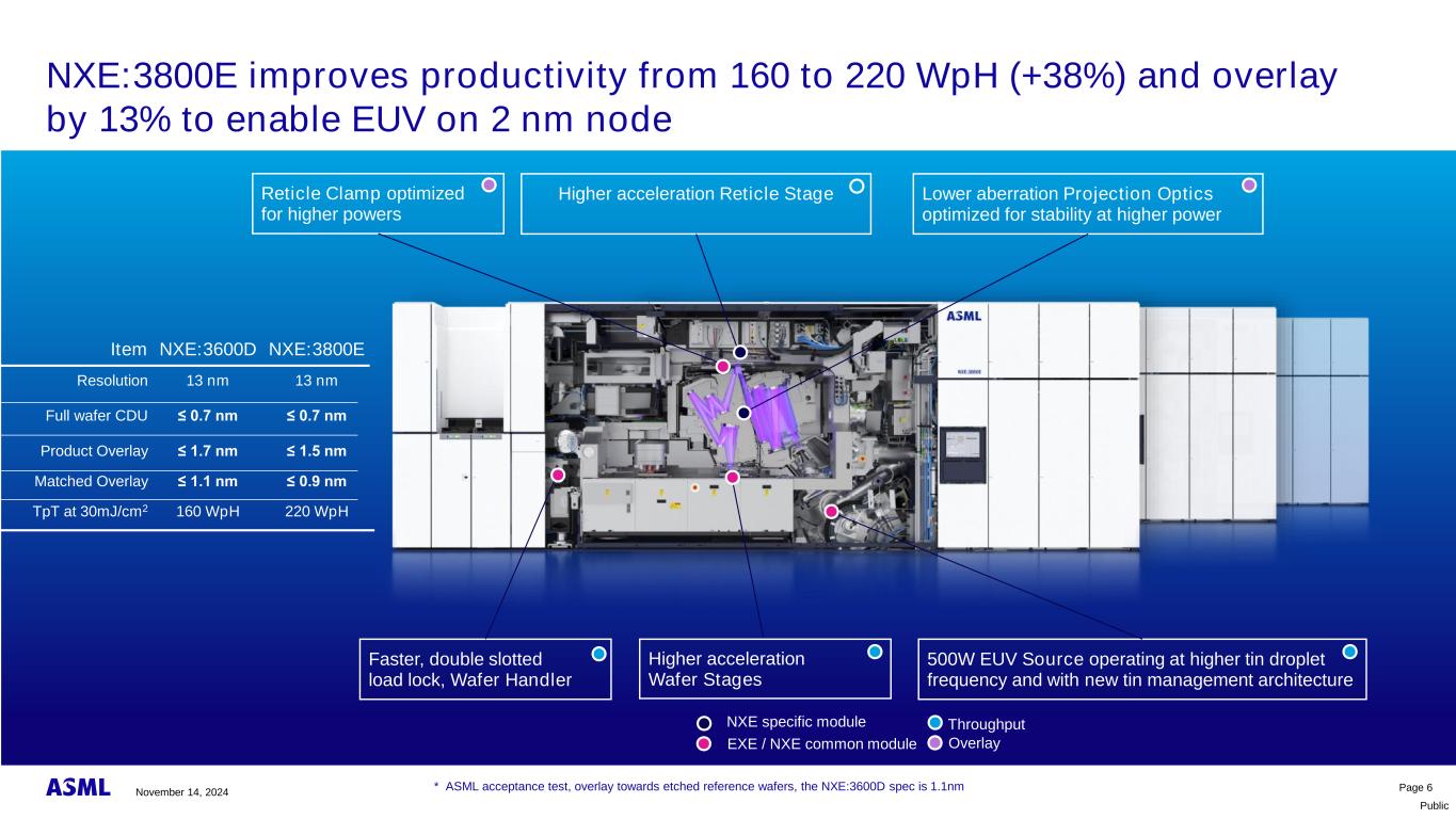
Public NXE:3800E improves productivity from 160 to 220 WpH (+38%) and overlay by 13% to enable EUV on 2 nm node Page 6 Higher acceleration Reticle Stage Lower aberration Projection Optics optimized for stability at higher power 500W EUV Source operating at higher tin droplet frequency and with new tin management architecture Faster, double slotted load lock, Wafer Handler Higher acceleration Wafer Stages Reticle Clamp optimized for higher powers EXE / NXE common module NXE specific module * ASML acceptance test, overlay towards etched reference wafers, the NXE:3600D spec is 1.1nm Item NXE:3600D NXE:3800E Resolution 13 nm 13 nm Full wafer CDU ≤ 0.7 nm ≤ 0.7 nm Product Overlay ≤ 1.7 nm ≤ 1.5 nm Matched Overlay ≤ 1.1 nm ≤ 0.9 nm TpT at 30mJ/cm2 160 WpH 220 WpH Overlay Throughput November 14, 2024
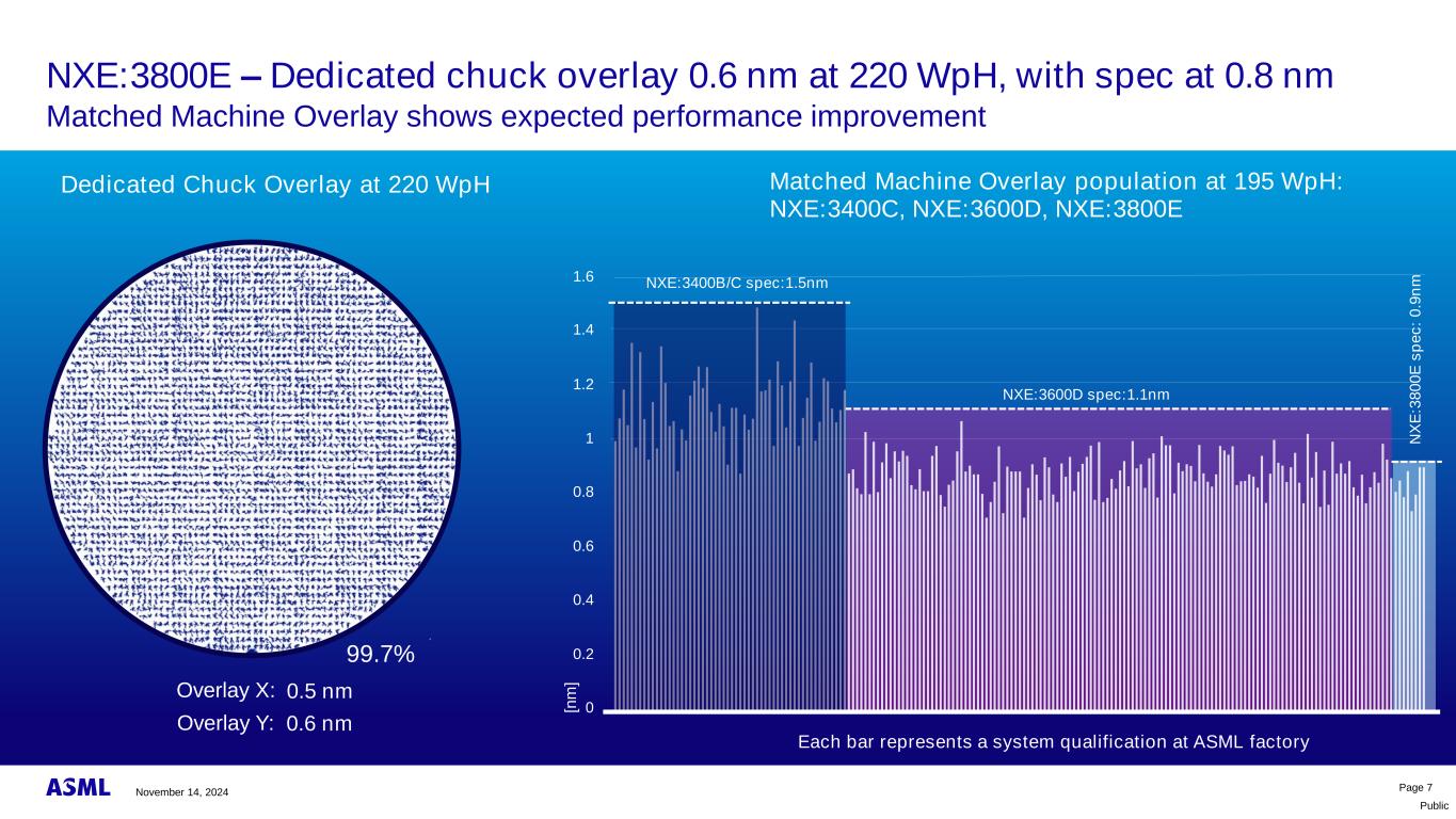
Public30-Sep-2024 | 0.33 NA EUV systems for high volume manufacturing. 13215-2 | slide 7 Dedicated Chuck Overlay at 220 WpH NXE:3800E – Dedicated chuck overlay 0.6 nm at 220 WpH, with spec at 0.8 nm Matched Machine Overlay shows expected performance improvement 1.6 1.4 1.2 1 0.8 0.6 0.4 0.2 0 Matched Machine Overlay population at 195 WpH: NXE:3400C, NXE:3600D, NXE:3800E NXE:3600D spec:1.1nm NXE:3400B/C spec:1.5nm N X E :3 8 0 0 E s p e c : 0 .9 n m [n m ] Each bar represents a system qualification at ASML factory Overlay X: Overlay Y: 99.7% 0.5 nm 0.6 nm November 14, 2024 Page 7

Public EUV customers are installing NXE:3800E at their R&D and HVM sites from 2024 NXE:3800 installed at DRAM, LOGIC and Foundry customers Page 8 JP TW KR US November 14, 2024
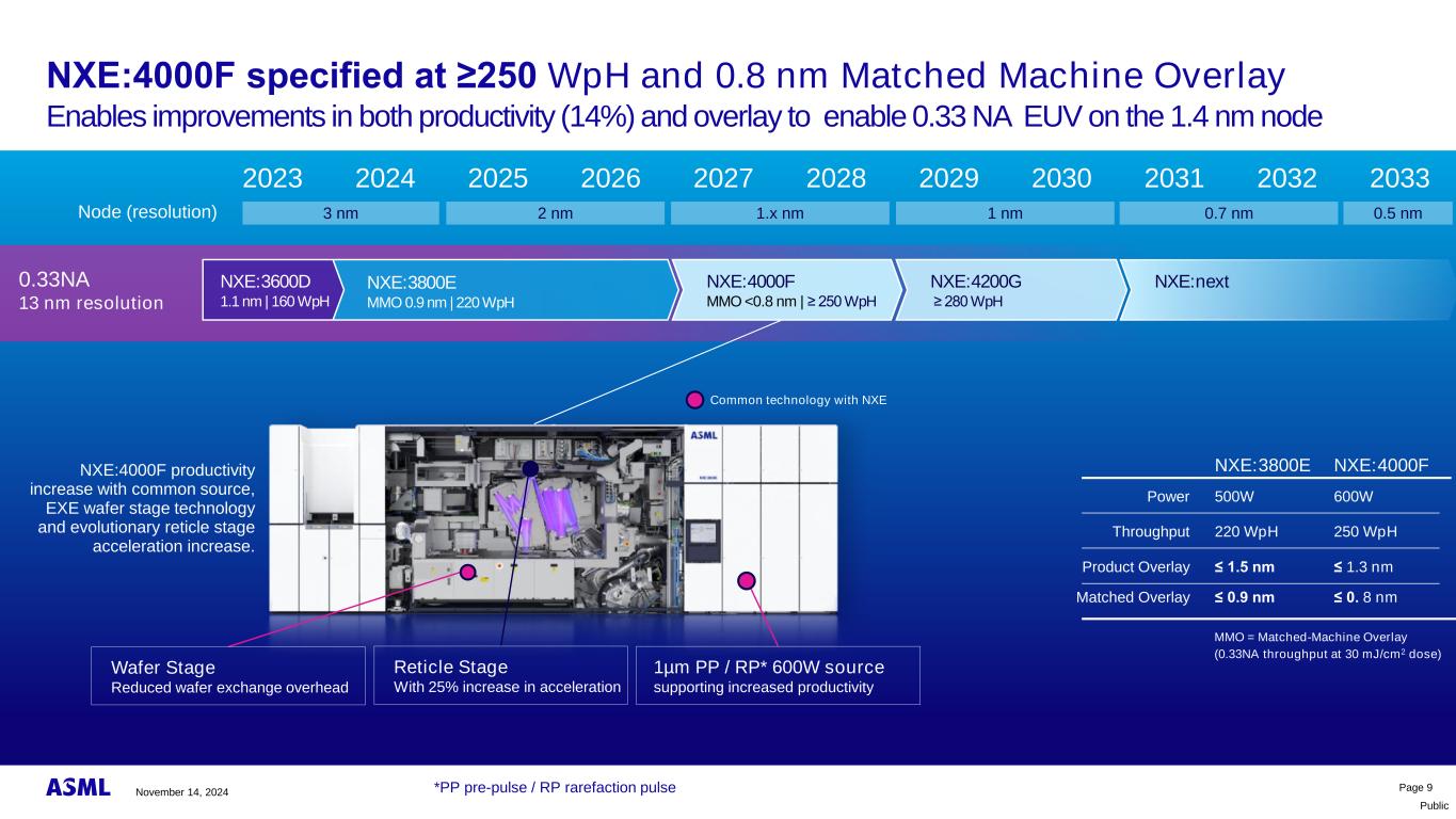
Public Page 9 2023 2024 2025 2026 2027 2028 2029 2030 2031 2032 2033 Node (resolution) 0.7 nm2 nm 1.x nm 1 nm3 nm 0.5 nm 0.33NA 13 nm resolution NXE:3600D 1.1 nm | 160 WpH NXE:3800E MMO 0.9 nm | 220 WpH NXE:4000F MMO <0.8 nm | ≥ 250 WpH NXE:4200G ≥ 280 WpH MMO = Matched-Machine Overlay (0.33NA throughput at 30 mJ/cm2 dose) Reticle Stage With 25% increase in acceleration 1µm PP / RP* 600W source supporting increased productivity Wafer Stage Reduced wafer exchange overhead NXE:3800E NXE:4000F Power 500W 600W Throughput 220 WpH 250 WpH Product Overlay ≤ 1.5 nm ≤ 1.3 nm Matched Overlay ≤ 0.9 nm ≤ 0. 8 nm NXE:4000F productivity increase with common source, EXE wafer stage technology and evolutionary reticle stage acceleration increase. Common technology with NXE NXE:next NXE:4000F specified at ≥250 WpH and 0.8 nm Matched Machine Overlay Enables improvements in both productivity (14%) and overlay to enable 0.33 NA EUV on the 1.4 nm node *PP pre-pulse / RP rarefaction pulse November 14, 2024
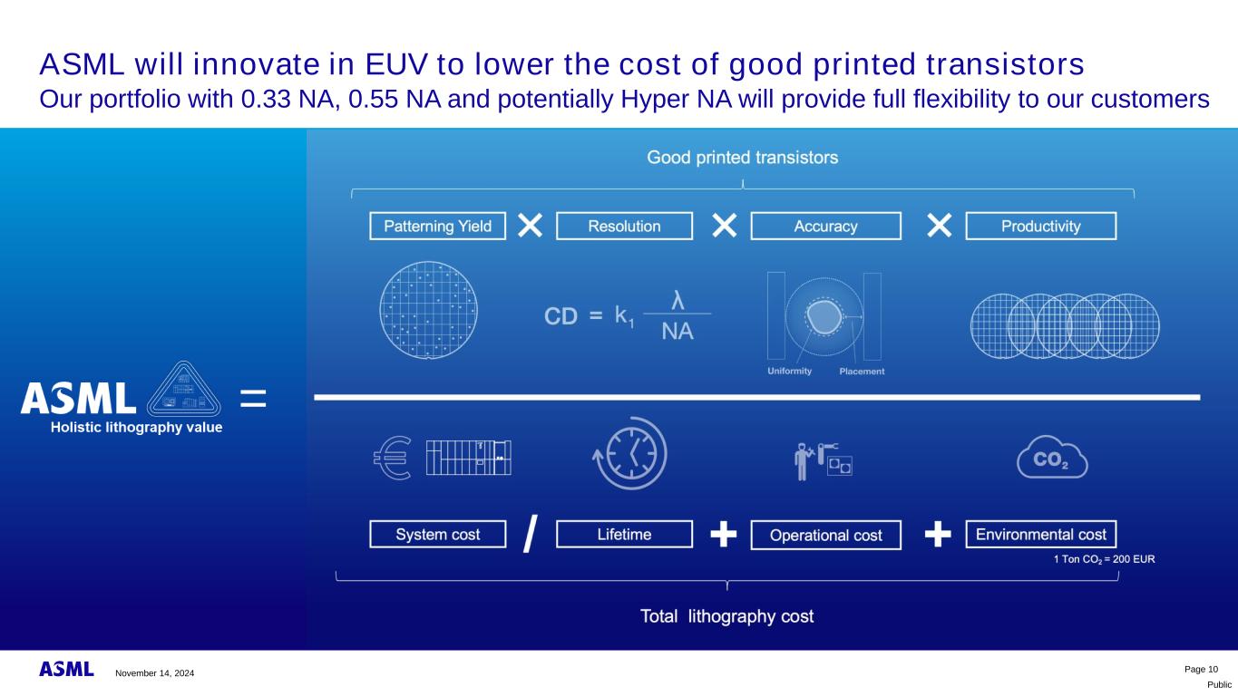
Public Good printed transistors Resolution ProductivityAccuracyPatterning Yield × × × Operational cost Environmental costSystem cost Lifetime/ + 1 Ton CO2 = 200 EUR + Total lithography cost ASML will innovate in EUV to lower the cost of good printed transistors Our portfolio with 0.33 NA, 0.55 NA and potentially Hyper NA will provide full flexibility to our customers Page 10 = November 14, 2024
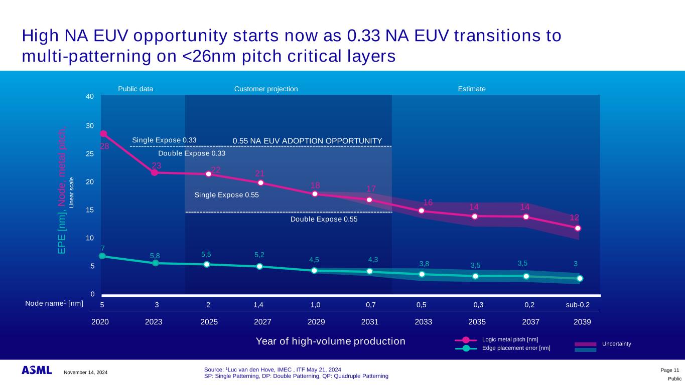
Public High NA EUV opportunity starts now as 0.33 NA EUV transitions to multi-patterning on <26nm pitch critical layers SP: Single Patterning, DP: Double Patterning, QP: Quadruple Patterning Source: 1Luc van den Hove, IMEC , ITF May 21, 2024 0 5 10 15 30 20 Single Expose 0.55 Double Expose 0.55 0.55 NA EUV ADOPTION OPPORTUNITYSingle Expose 0.33 Double Expose 0.3325 21 18 16 14 28 5,2 4,3 3,5 3,5 Public data Customer projection Estimate 2020 2023 2025 2027 2029 2031 2033 2035 17 14 3,8 22 23 E P E [ n m ], N o d e , m e ta l p it c h , L in e a r s c a le Year of high-volume production 7 20392037 12 3 5 3 2 1,4 1,0 0,7 0,20,5 0,3 sub-0.2 Logic metal pitch [nm] Edge placement error [nm] Uncertainty 5,5 4,5 5,8 Node name1 [nm] 40 Page 11November 14, 2024
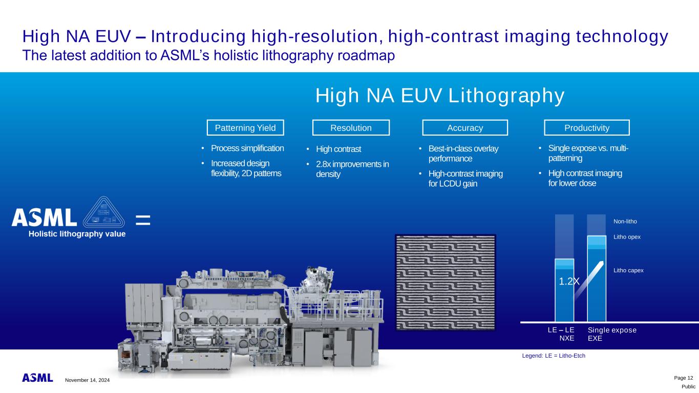
Public High NA EUV – Introducing high-resolution, high-contrast imaging technology The latest addition to SML’s holistic lithography roadmap High NA EUV Lithography • Best-in-class overlay performance • High-contrast imaging for LCDU gain • Single expose vs. multi- patterning • High contrast imaging for lower dose • High contrast • 2.8x improvements in density • Process simplification • Increased design flexibility, 2D patterns Resolution ProductivityAccuracyPatterning Yield = Single expose EXE LE – LE NXE Non-litho Litho opex Litho capex Legend: LE = Litho-Etch 1.2X Page 12November 14, 2024
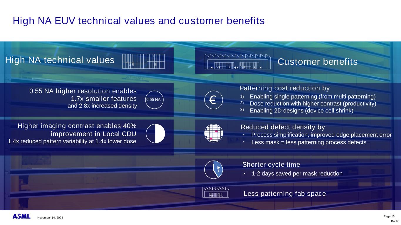
Public High NA EUV technical values and customer benefits Page 13 Customer benefitsHigh NA technical values Less mask = less patterning process defects Process simplification, improved edge placement error Reduced defect density by Patterning cost reduction by Enabling single patterning (from multi patterning) Dose reduction with higher contrast (productivity) Enabling 2D designs (device cell shrink) 1) 2) 3) 1-2 days saved per mask reduction Shorter cycle time Less patterning fab space 0.55 NA higher resolution enables 1.7x smaller features and 2.8x increased density Higher imaging contrast enables 40% improvement in Local CDU 1.4x reduced pattern variability at 1.4x lower dose 0 55 November 14, 2024
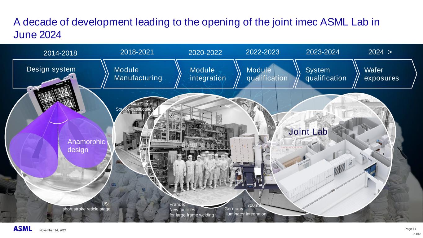
Public A decade of development leading to the opening of the joint imec ASML Lab in June 2024 France: milling body US: short stroke reticle stage Netherlands: 700m2 High-NA assembly building openedFrance: New facilities for large frame welding Germany: New facilities for optic metrology Module integration 2020-2022 Module qualification 2022-2023 2023-2024 System qualification 2024 > Wafer exposures 2018-2021 Module Manufacturing Design system 2014-2018 Anamorphic design San Diego: Source qualification Germany Illuminator integration Veldhoven: qualification waferstage Wilton: qualification reticlestage Veldhoven System integration Joint Lab Page 14November 14, 2024
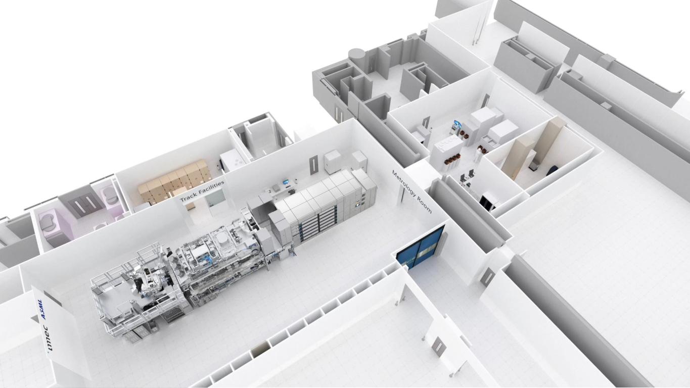
Public Litho Cluster: system install ongoing and track qualified High NA scanner Metrology Room Track IMEC / ASML High NA Lab supporting future insertion High NA lab provides early access to all EUV customers Page 15 Public
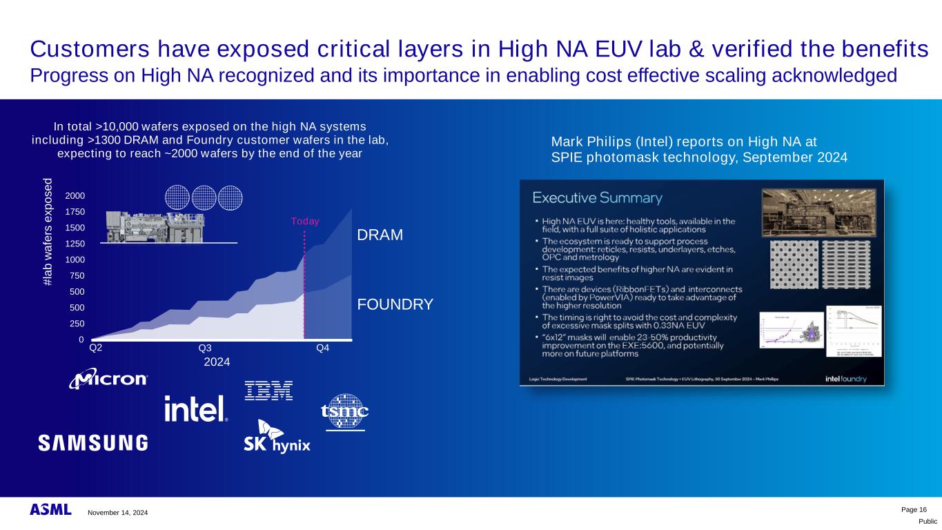
Public Customers have exposed critical layers in High NA EUV lab & verified the benefits Progress on High NA recognized and its importance in enabling cost effective scaling acknowledged Page 16 Mark Philips (Intel) reports on High NA at SPIE photomask technology, September 2024 In total >10,000 wafers exposed on the high NA systems including >1300 DRAM and Foundry customer wafers in the lab, expecting to reach ~2000 wafers by the end of the year 2000 1750 1500 1250 1000 750 500 500 250 0 Q2 Q3 Q4 Today # la b w a fe rs e x p o s e d 2024 DRAM FOUNDRY November 14, 2024
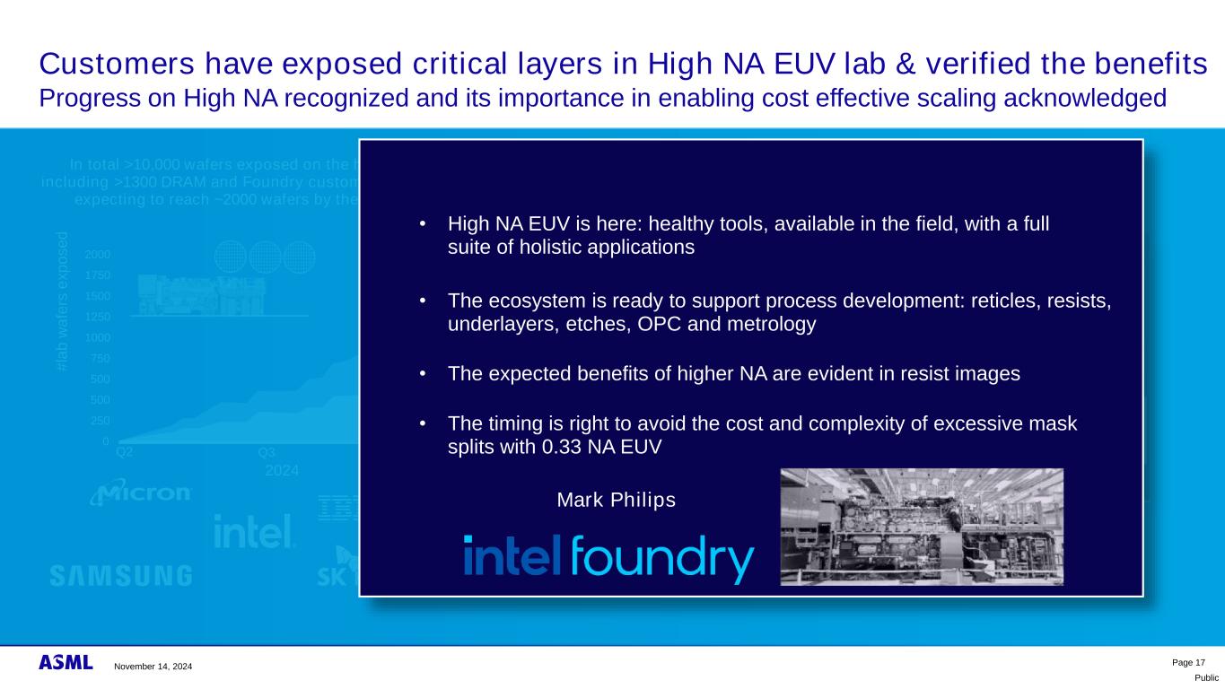
Public In total >10,000 wafers exposed on the high NA systems including >1300 DRAM and Foundry customer wafers in the lab, expecting to reach ~2000 wafers by the end of the year 2000 1750 1500 1250 1000 750 500 500 250 0 Q2 Q3 Q4 Today # la b w a fe rs e x p o s e d 2024 DRAM FOUNDRY Customers have exposed critical layers in High NA EUV lab & verified the benefits Progress on High NA recognized and its importance in enabling cost effective scaling acknowledged Page 17 Mark Philips (Intel) reports on High NA at SPIE photomask technology, September 2024 • High NA EUV is here: healthy tools, available in the field, with a full suite of holistic applications • The ecosystem is ready to support process development: reticles, resists, underlayers, etches, OPC and metrology • The expected benefits of higher NA are evident in resist images • The timing is right to avoid the cost and complexity of excessive mask splits with 0.33 NA EUV Mark Philips November 14, 2024
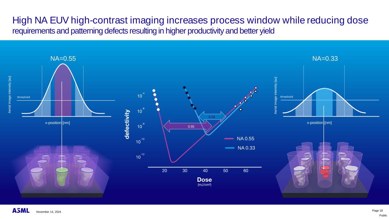
Public High NA EUV high-contrast imaging increases process window while reducing dose requirements and patterning defects resulting in higher productivity and better yield x-position [nm] threshold NA=0.55 x-position [nm] A e ri a l im a g e i n te n s it y [ a u ] NA=0.33 threshold 0.33 0.55 Page 18 NA 0.55 NA 0.33 A e ri a l im a g e i n te n s it y [ a u ] November 14, 2024
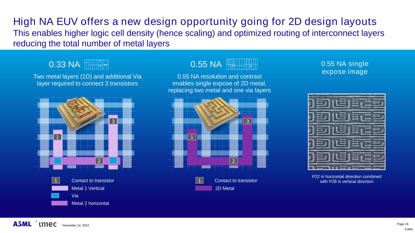
Public High NA EUV offers a new design opportunity going for 2D design layouts This enables higher logic cell density (hence scaling) and optimized routing of interconnect layers reducing the total number of metal layers Page 19 0.33 NA 0.55 NA 0.55 NA resolution and contrast enables single expose of 2D metal, replacing two metal and one via layers Two metal layers (1D) and additional Via layer required to connect 3 transistors P22 in horizontal direction combined with P28 in vertical direction 0.55 NA single expose image Metal 1 Vertical Metal 2 horizontal Via 1 3 2 1 2D Metal Contact to transistor 1 3 2 Contact to transistor1 November 14, 2024
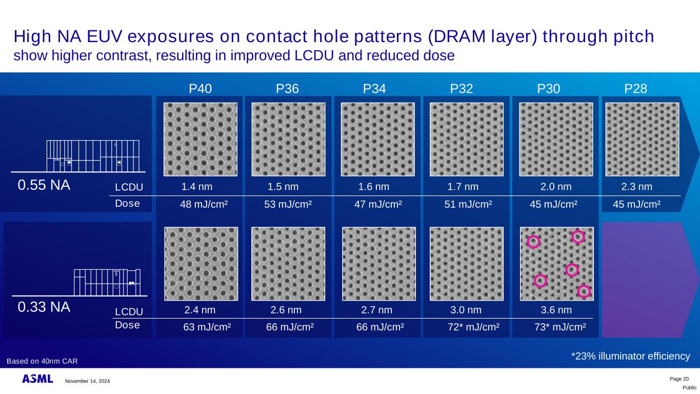
Public High NA EUV exposures on contact hole patterns (DRAM layer) through pitch show higher contrast, resulting in improved LCDU and reduced dose Page 20 P40 P36 P34 P32 P30 0.33 NA 0.55 NA LCDU Dose LCDU Dose 2.4 nm 2.6 nm 2.7 nm 3.0 nm 3.6 nm 63 mJ/cm² 66 mJ/cm² 66 mJ/cm² 72* mJ/cm² 73* mJ/cm² Based on 40nm CAR P28 1.4 nm 1.5 nm 1.6 nm 1.7 nm 2.0 nm 48 mJ/cm² 53 mJ/cm² 47 mJ/cm² 51 mJ/cm² 45 mJ/cm² 2.3 nm 45 mJ/cm² *23% illuminator efficiency November 14, 2024

Public High NA EUV exposures on contact hole patterns (DRAM layer) through pitch show higher contrast, resulting in improved LCDU and reduced dose Page 21 P40 P36 P34 P32 P30 0.33 NA 0.55 NA LCDU Dose LCDU 2.4 nm 2.6 nm 2.7 nm 3.0 nm 3.6 nm Based on 40nm CAR P28 1.4 nm 1.5 nm 1.6 nm 1.7 nm 2.0 nm 48 mJ/cm² 53 mJ/cm² 47 mJ/cm² 51 mJ/cm² 45 mJ/cm² 2.3 nm 45 mJ/cm² Dose at same LCDU as 0.55 NA 191 mJ/cm² 209 mJ/cm² 193 mJ/cm² 220* mJ/cm² 238* mJ/cm² *23% illuminator efficiency November 14, 2024
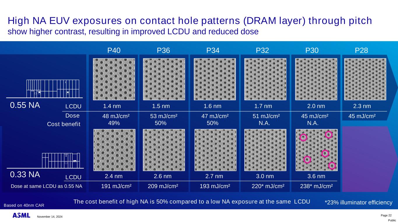
Public High NA EUV exposures on contact hole patterns (DRAM layer) through pitch show higher contrast, resulting in improved LCDU and reduced dose Page 22 P40 P36 P34 P32 P30 0.33 NA 0.55 NA LCDU Dose LCDU 2.4 nm 2.6 nm 2.7 nm 3.0 nm 3.6 nm Based on 40nm CAR P28 1.4 nm 1.5 nm 1.6 nm 1.7 nm 2.0 nm 48 mJ/cm² 53 mJ/cm² 47 mJ/cm² 51 mJ/cm² 45 mJ/cm² 2.3 nm 45 mJ/cm² Dose at same LCDU as 0.55 NA The cost benefit of high NA is 50% compared to a low NA exposure at the same LCDU Cost benefit 49% 50% 50% N.A. N.A. 191 mJ/cm² 209 mJ/cm² 193 mJ/cm² 220* mJ/cm² 238* mJ/cm² *23% illuminator efficiency November 14, 2024
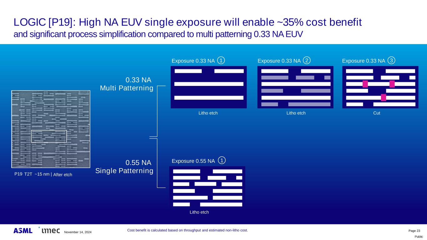
Public LOGIC [P19]: High NA EUV single exposure will enable ~35% cost benefit and significant process simplification compared to multi patterning 0.33 NA EUV Page 23 Exposure 0.55 NA Litho etch 0.33 NA Multi Patterning 0.55 NA Single Patterning Exposure 0.33 NA 1 Exposure 0.33 NA 2 Exposure 0.33 NA 3 Litho etch Litho etch Cut T2T ~15 nm | After etchP19 1 Cost benefit is calculated based on throughput and estimated non-litho cost. November 14, 2024
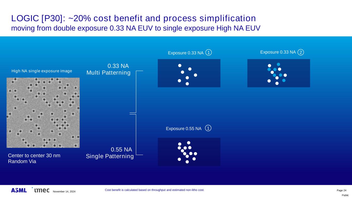
Public LOGIC [P30]: ~20% cost benefit and process simplification moving from double exposure 0.33 NA EUV to single exposure High NA EUV Page 24 Center to center 30 nm Random Via 0.33 NA Multi Patterning 0.55 NA Single Patterning Exposure 0.55 NA 1 High NA single exposure image Exposure 0.33 NA 1 Exposure 0.33 NA 2 Cost benefit is calculated based on throughput and estimated non-litho cost. November 14, 2024
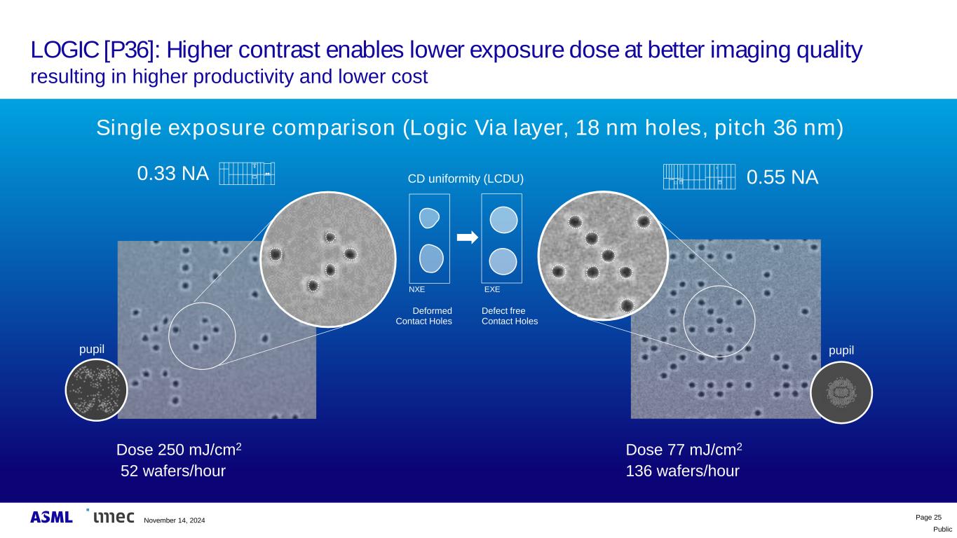
Public LOGIC [P36]: Higher contrast enables lower exposure dose at better imaging quality resulting in higher productivity and lower cost Page 25 Single exposure comparison (Logic Via layer, 18 nm holes, pitch 36 nm) 0.33 NA CD uniformity (LCDU) NXE EXE Deformed Contact Holes Defect free Contact Holes 0.55 NA Dose 250 mJ/cm2 52 wafers/hour pupil pupil Dose 77 mJ/cm2 136 wafers/hour November 14, 2024
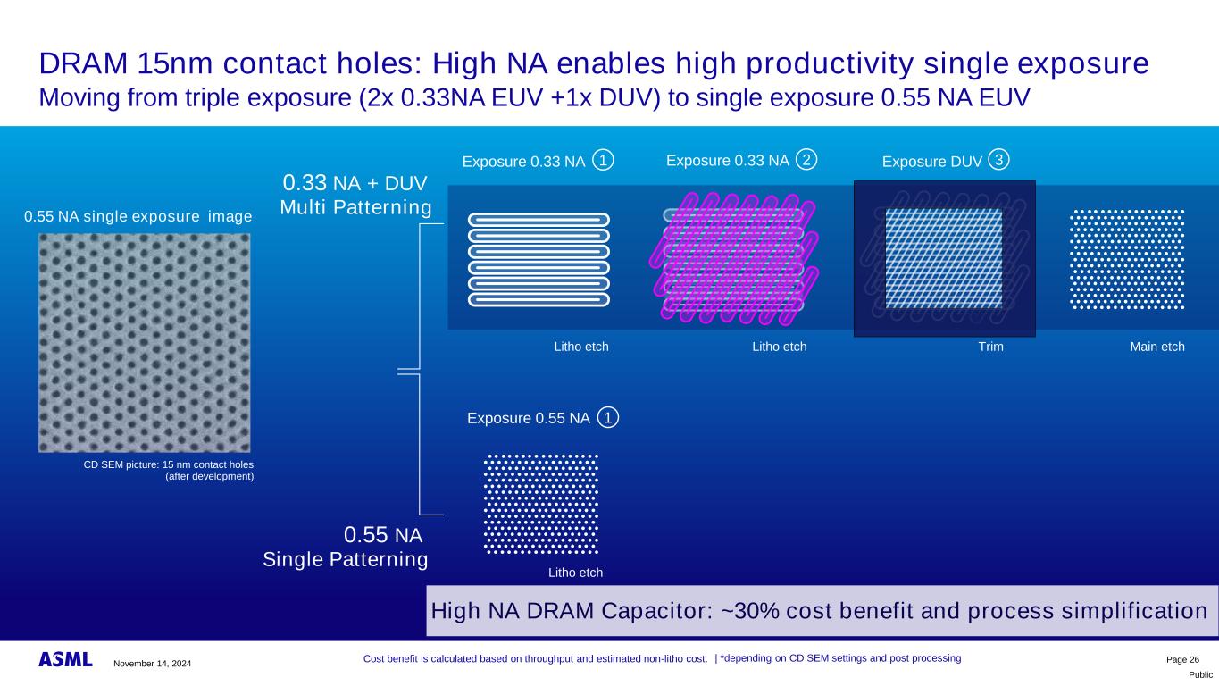
Public DRAM 15nm contact holes: High NA enables high productivity single exposure Moving from triple exposure (2x 0.33NA EUV +1x DUV) to single exposure 0.55 NA EUV Page 26 CD SEM picture: 15 nm contact holes (after development) 0.33 NA + DUV Multi Patterning 0.55 NA Single Patterning Exposure 0.33 NA 1 Exposure 0.33 NA 2 Exposure DUV 3 Exposure 0.55 NA 1 Litho etch 0.55 NA single exposure image Cost benefit is calculated based on throughput and estimated non-litho cost. | *depending on CD SEM settings and post processing Litho etch Litho etch Trim Main etch High NA DRAM Capacitor: ~30% cost benefit and process simplification November 14, 2024
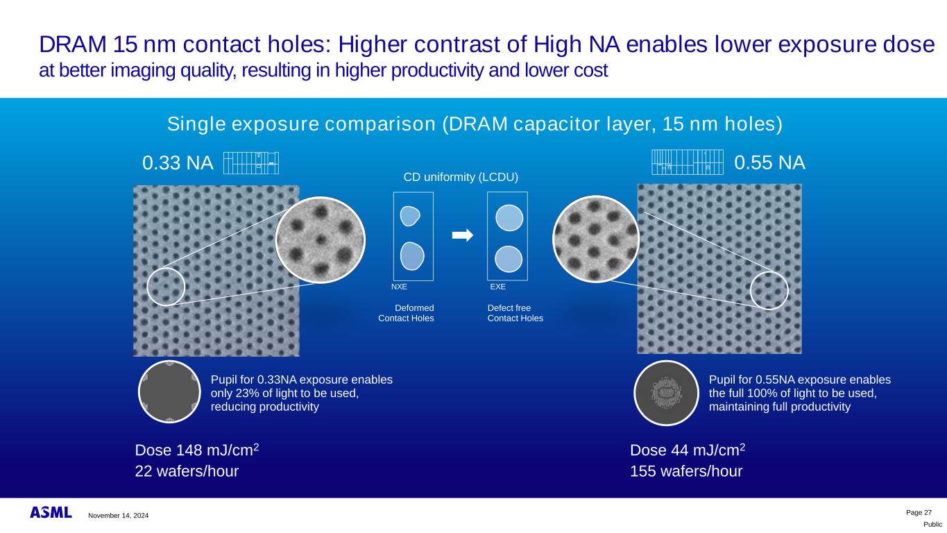
Public DRAM 15 nm contact holes: Higher contrast of High NA enables lower exposure dose at better imaging quality, resulting in higher productivity and lower cost Page 27 Single exposure comparison (DRAM capacitor layer, 15 nm holes) 0.33 NA CD uniformity (LCDU) NXE EXE Pupil for 0.33NA exposure enables only 23% of light to be used, reducing productivity Deformed Contact Holes Defect free Contact Holes 0.55 NA Pupil for 0.55NA exposure enables the full 100% of light to be used, maintaining full productivity Dose 148 mJ/cm2 22 wafers/hour Dose 44 mJ/cm2 155 wafers/hour November 14, 2024
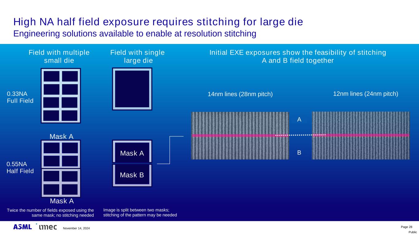
Public High NA half field exposure requires stitching for large die Engineering solutions available to enable at resolution stitching Page 28 14nm lines (28nm pitch) 12nm lines (24nm pitch) Initial EXE exposures show the feasibility of stitching A and B field together 0.33NA Full Field 0.55NA Half Field Field with multiple small die Mask A Mask B Field with single large die Twice the number of fields exposed using the same mask; no stitching needed Image is split between two masks; stitching of the pattern may be needed Mask A Mask A B A November 14, 2024
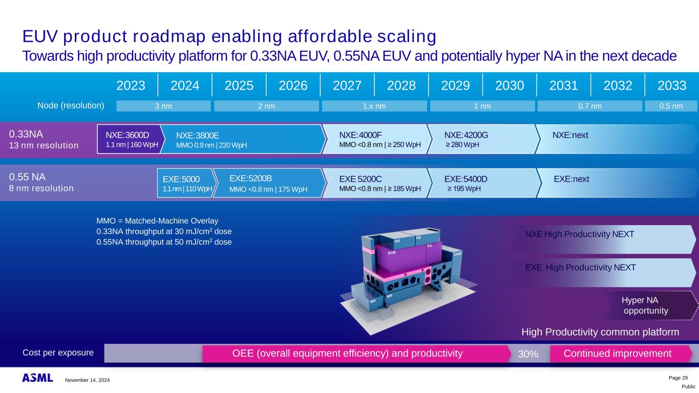
Public EUV product roadmap enabling affordable scaling Towards high productivity platform for 0.33NA EUV, 0.55NA EUV and potentially hyper NA in the next decade Page 29 2023 2024 2025 2026 2027 2028 2029 2030 2031 2032 2033 Node (resolution) 0.7 nm2 nm 1.x nm 1 nm3 nm 0.5 nm 0.55 NA 8 nm resolution EXE:5200B MMO <0.8 nm | 175 WpH EXE:5000 1.1 nm | 110 WpH EXE 5200C MMO <0.8 nm | ≥ 185 WpH EXE:5400D ≥ 95 WpH EXE High Productivity NEXT NXE High Productivity NEXT Hyper NA opportunity High Productivity common platform 30%Cost per exposure MMO = Matched-Machine Overlay 0.33NA throughput at 30 mJ/cm2 dose 0.55NA throughput at 50 mJ/cm2 dose 0.33NA 13 nm resolution NXE:3600D 1.1 nm | 160 WpH NXE:3800E MMO 0.9 nm | 220 WpH NXE:4000F MMO <0.8 nm | ≥ 250 WpH NXE:4200G ≥ 280 WpH NXE:next EXE:next OEE (overall equipment efficiency) and productivity Continued improvement November 14, 2024
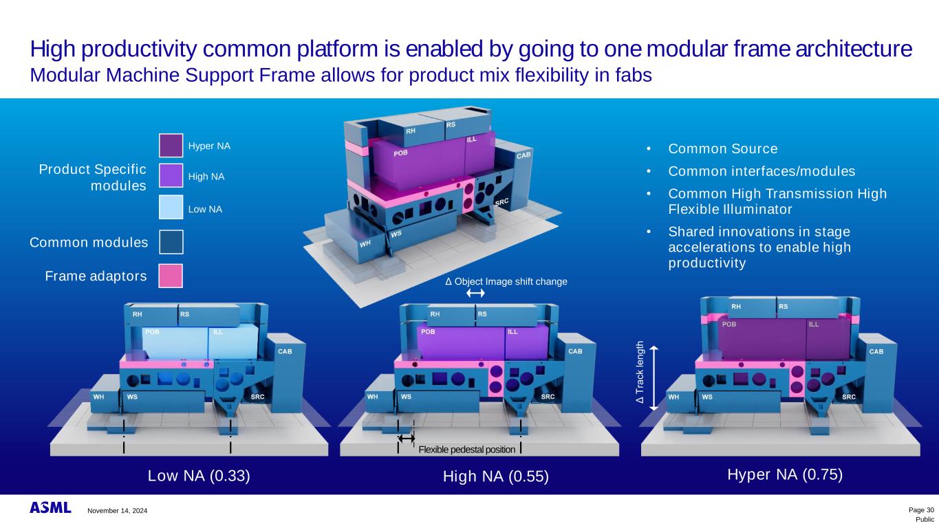
Public High productivity common platform is enabled by going to one modular frame architecture Modular Machine Support Frame allows for product mix flexibility in fabs • Common Source • Common interfaces/modules • Common High Transmission High Flexible Illuminator • Shared innovations in stage accelerations to enable high productivity Low NA (0.33) Common modules Product Specific modules Low NA Frame adaptors High NA (0.55) Flexible pedestal position High NA Hyper NA (0.75) Δ T ra c le n g th Hyper NA Δ Object Image shift change Page 30November 14, 2024
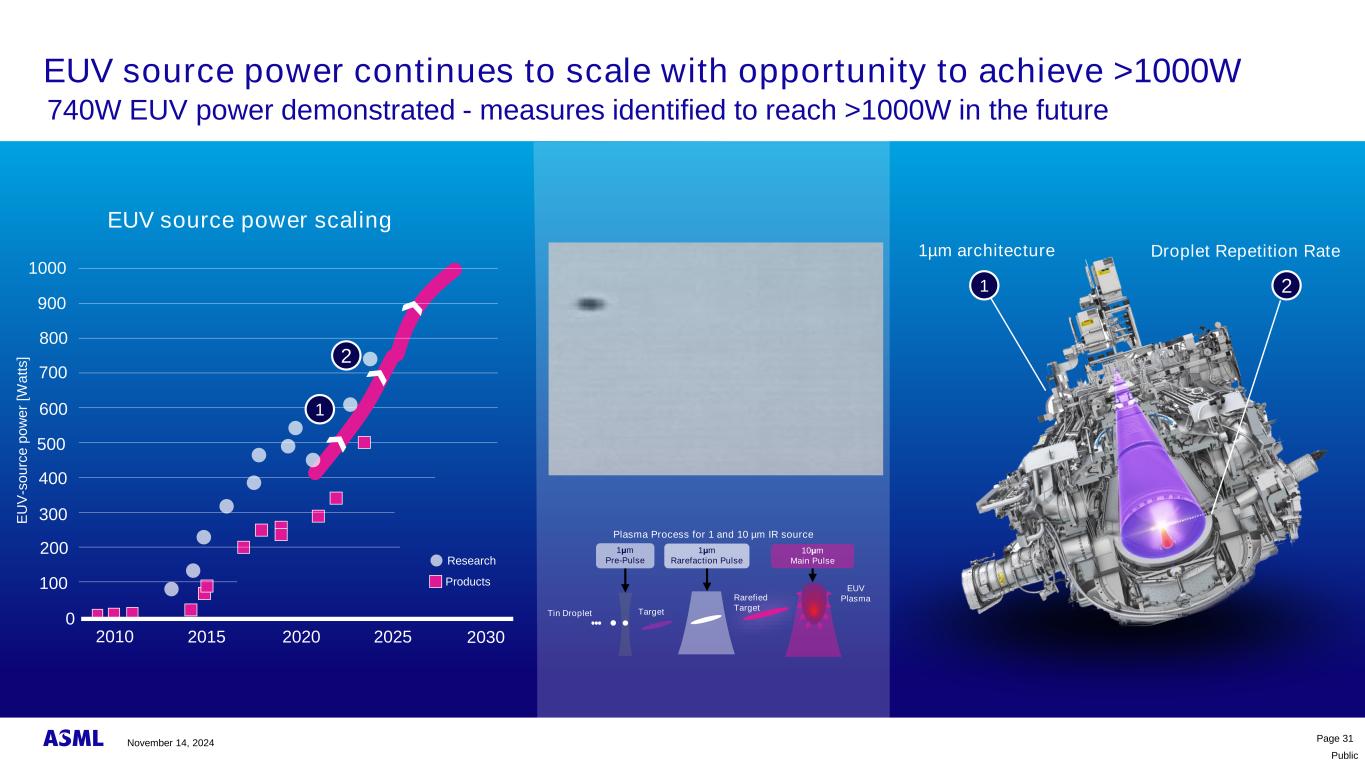
Public EUV source power continues to scale with opportunity to achieve >1000W 740W EUV power demonstrated - measures identified to reach >1000W in the future EUV source power scaling 2010 2015 2020 2025 0 100 200 300 400 500 600 E U V -s o u rc e p o w e r [W a tt s ] Products 2030 700 800 900 1000 1 2 Research 1 EUV Plasma 1μm Pre-Pulse 1μm Rarefaction Pulse 10μm Main Pulse 2 Plasma Process for 1 and 10 µm IR source Target Rarefied Target Tin Droplet 1µm architecture Droplet Repetition Rate Page 31November 14, 2024
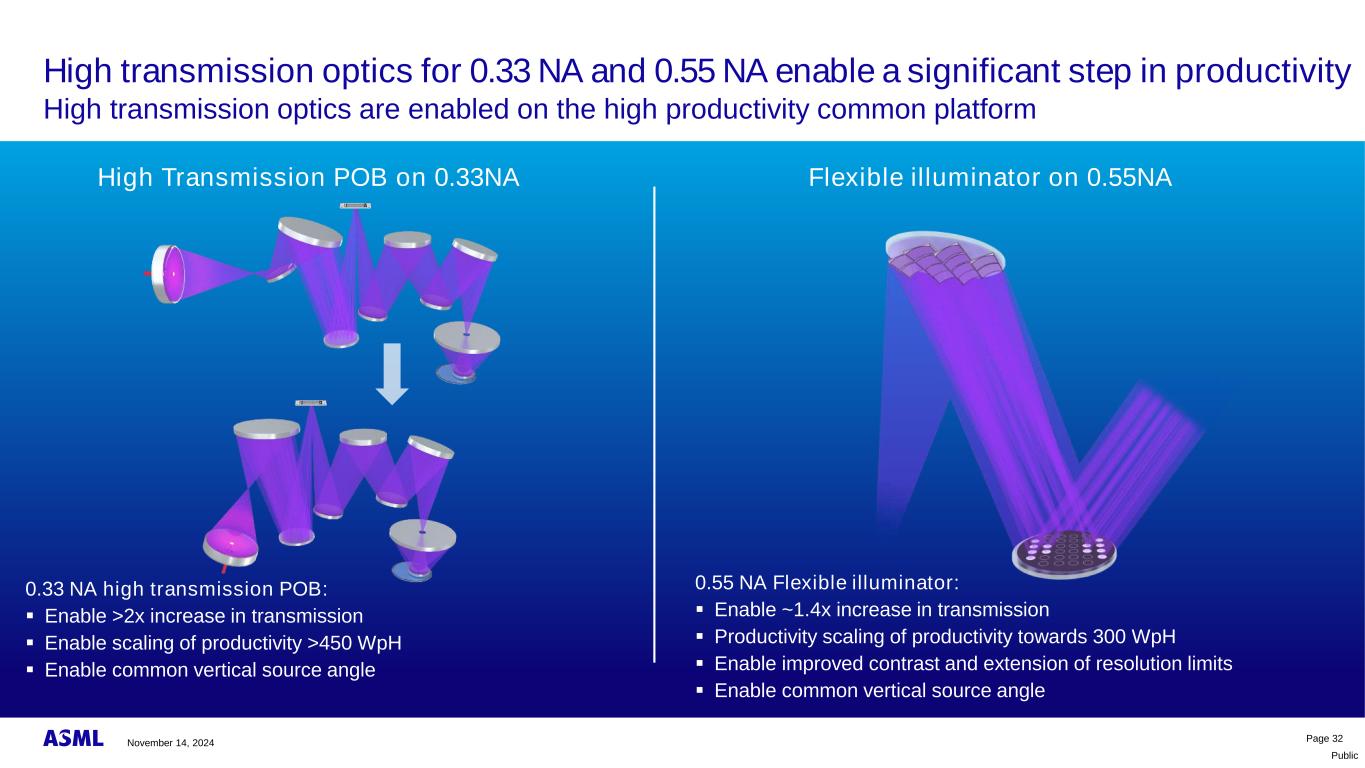
Public High transmission optics for 0.33 NA and 0.55 NA enable a significant step in productivity High transmission optics are enabled on the high productivity common platform Page 32 0.55 NA Flexible illuminator: ▪ Enable ~1.4x increase in transmission ▪ Productivity scaling of productivity towards 300 WpH ▪ Enable improved contrast and extension of resolution limits ▪ Enable common vertical source angle High Transmission POB on 0.33NA Flexible illuminator on 0.55NA 0.33 NA high transmission POB: ▪ Enable >2x increase in transmission ▪ Enable scaling of productivity >450 WpH ▪ Enable common vertical source angle November 14, 2024
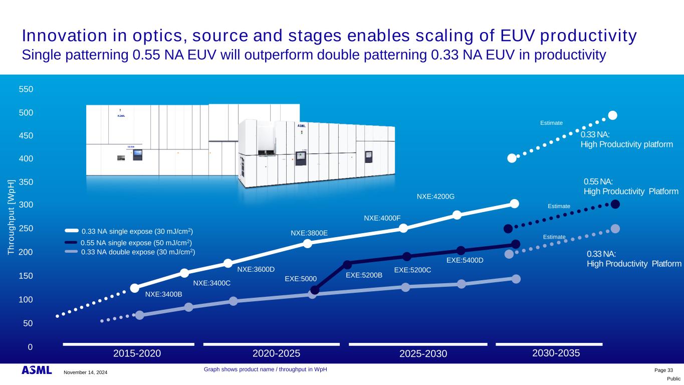
Public Innovation in optics, source and stages enables scaling of EUV productivity Single patterning 0.55 NA EUV will outperform double patterning 0.33 NA EUV in productivity Page 33Graph shows product name / throughput in WpH 500 550 450 400 350 300 250 T h ro u g h p u t [W p H ] 200 150 100 50 0 2015-2020 2020-2025 2030-20352025-2030 NXE:3400B NXE:3400C NXE:3600D NXE:3800E NXE:4000F NXE:4200G 0.33 NA single expose (30 mJ/cm2) 0.33 NA: High Productivity platform Estimate 0.33 NA double expose (30 mJ/cm2) 0.55 NA single expose (50 mJ/cm2) 0.55 NA: High Productivity Platform EXE:5000 EXE:5200B EXE:5400D EXE:5200C 0.33 NA: High Productivity Platform Estimate Estimate November 14, 2024
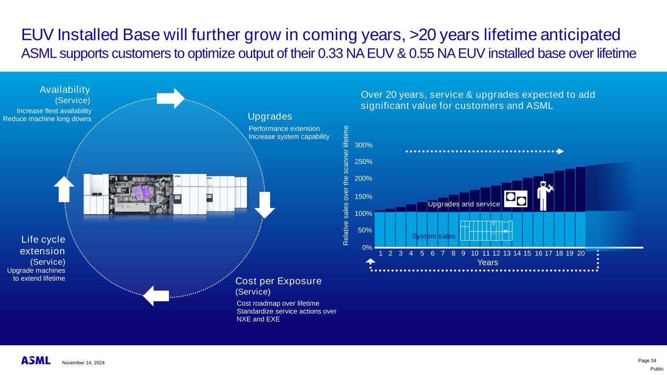
Public EUV Installed Base will further grow in coming years, >20 years lifetime anticipated ASML supports customers to optimize output of their 0.33 NA EUV & 0.55 NA EUV installed base over lifetime Page 34 Availability (Service) Life cycle extension (Service) Upgrades Cost per Exposure (Service) Increase fleet availability Reduce machine long downs Performance extension Increase system capability Cost roadmap over lifetime Standardize service actions over NXE and EXE Upgrade machines to extend lifetime R e la ti v e s a le s o v e r th e s c a n n e r lif e ti m e 1 2 3 4 5 6 7 8 9 10 11 12 13 14 15 16 17 18 19 20 0% 50% 100% 150% 200% 250% Years Upgrades and service System sales 300% Over 20 years, service & upgrades expected to add significant value for customers and ASML November 14, 2024

Public Key messages • EUV has reached high-volume manufacturing maturity providing a solid foundation for continued innovation. • The NXE:3800E offers a 38% improvement in productivity and 13% in overlay, with additional productivity and overlay improvements planned for the NXE:4000F and beyond. • The imec ASML High NA EUV lab opened in June, and all EUV customers have exposed critical layers. The data prove the capability of the system in lowering costs by 20-35% for critical layers compared to 0.33 NA, by dose reduction, enabling single exposure and 2D layout designs. • The first High NA EUV systems are operational at a customer, marking a key milestone in adoption of High NA EUV. • In the future both 0.33 NA and 0.55 NA EUV systems will be used for critical exposures. The EUV roadmap for the next decade includes the introduction of a high productivity platform and will enable affordable scaling for both 0.33 NA, 0.55 NA and potentially Hyper NA. • The growing installed base opportunity will be leveraged with a value- based service model in combination with productivity and performance upgrades.

Public Forward Looking Statements This document and related discussions contain statements that are forward-looking within the meaning of the U.S. Private Securities Litigation Reform Act of 1995, including statements with respect to our strategy, plans and expected trends, including trends in end markets and the technology industry and business environment trends, including the emergence of AI and its potential opportunities and expectations for the semiconductor industry, including computing power, advanced logic nodes and R M memory, statements with respect to Moore’s law and expected transistor growth and aspirations by 2030, global market trends and technology, product and customer roadmaps, long term outlook and expected lithography and semiconductor industry growth and trends and expected growth in semiconductor sales and semiconductor market opportunity through to 2030 and beyond, expected growth in wafer demand and capacity and additional wafer capacity requirements, expected investments by our customers, including investments in our technology and in wafer capacity, plans to increase capacity, expected growth in lithography spend, growth opportunities including opportunities for growth in service and upgrades and opportunities for growth in Installed Base Management sales, expected growth and gross margins in the holistic lithography business and expected addressable mar et for pplications products, expectations and benefits of a growing installed base, SML’s and its supplier’s capacity, expected production of systems, model scenarios and the updated model for 2030, including annual revenue and gross margin opportunity and development potential for 2030, outlook and expected, modelled or potential financial results, including revenue opportunity, gross margin, R&D costs, SG&A costs, capital expenditure, cash conversion cycle and annualized effective tax rate for 2030 and assumptions and drivers underlying such expected, modelled or potential amounts, and other assumptions underlying our business and financial models, expected trends, outlook and growth in semiconductor end markets and long term growth opportunities, demand and demand drivers, expected opportunities and growth drivers for and technological innovation of our products including DUV EUV, High NA, Hyper NA, Applications, and other products impacting productivity and costs, transistor dimensions, logic and DRAM shrink, foundry competition, statements with respect to dividends and share buybacks and our capital return policy, including expectation to return significant amounts of cash to shareholders through growing dividends and buybacks and statements with respect to energy generation and consumption trends and the drive toward energy efficiency, emissions reduction and greenhouse gas neutrality goals and target dates to achieve greenhouse gas neutrality, zero waste from operations and other ESG targets and ambitions and plans to maintain a leadership position in ESG, increasing technological sovereignty across the world and the expected impact on semiconductor sales, including specific goals of countries across the world, increasing competition in the foundry business, estimates for 2024 and other non-historical statements. You can generally identify these statements by the use of words like "may", "will", "could", "should", "project", "believe", "anticipate", "expect", "plan", "estimate", "forecast", "potential", “opportunity”, “scenario”, “guidance,” "intend", "continue", "target", "future", "progress", "goal" and variations of these words or comparable words. These statements are not historical facts, but rather are based on current expectations, estimates, assumptions, models, opportunities and projections about our business and our future and potential financial results and readers should not place undue reliance on them. Forward- looking statements do not guarantee future performance and involve a number of substantial known and unknown risks and uncertainties. These risks and uncertainties include, without limitation, customer demand, semiconductor equipment industry capacity, worldwide demand for semiconductors and semiconductor manufacturing capacity, lithography tool utilization and semiconductor inventory levels, general trends and consumer confidence in the semiconductor industry and end markets, the impact of general economic conditions, including the impact of the current macroeconomic environment on the semiconductor industry, uncertainty around a market recovery including the timing thereof, the impact of inflation, interest rates, wars and geopolitical developments, the impact of pandemics, the performance of our systems, the success of technology advances and the pace of new product development and customer acceptance of and demand for new products, our production capacity and ability to adjust capacity to meet demand, supply chain capacity, timely availability of parts and components, raw materials, critical manufacturing equipment and qualified employees, our ability to produce systems to meet demand, the number and timing of systems ordered, shipped and recognized in revenue, risks relating to fluctuations in net bookings and our ability to convert bookings into sales, the risk of order cancellation or push outs and restrictions on shipments of ordered systems under export controls, ris s relating to technology, product and customer roadmaps and Moore’s law, risks relating to the trade environment, import/export and national security regulations and orders and their impact on us, including the impact of changes in export regulations and the impact of such regulations on our ability to obtain necessary licenses and to sell our systems and provide services to certain customers, exchange rate fluctuations, changes in tax rates, available liquidity and free cash flow and liquidity requirements, our ability to refinance our indebtedness, available cash and distributable reserves for, and other factors impacting, dividend payments and share repurchases, the number of shares that we repurchase under our share repurchase programs, our ability to enforce patents and protect intellectual property rights and the outcome of intellectual property disputes and litigation, our ability to meet ESG goals and execute our ESG strategy, other factors that may impact SML’s business or financial results including the risk that actual results may differ materially from the models, potential and opportunity we present for 2030 and other future periods, and other ris s indicated in the ris factors included in SML’s nnual Report on Form 20-F for the year ended December 31, 2023 and other filings with and submissions to the US Securities and Exchange Commission. These forward-looking statements are made only as of the date of this document. We undertake no obligation to update any forward-looking statements after the date of this report or to conform such statements to actual results or revised expectations, except as required by law. This document and related discussions contain statements relating to our approach to and interim progress on achieving certain energy efficiency and greenhouse gas emissions reduction targets, including our ambition to achieve greenhouse gas neutrality References to “greenhouse gas neutral” means remaining emissions, after SML’s efforts to reach its GHG emission reduction targets, compensated by the same amount of metric tons of carbon credits that are verified against recognised quality standards. Page 36November 14, 2024

Public THANK YOU